Prominent semiconductor companies have started and declared programs to build US-based fabs, and others are being planned. DeepTech can help you proceed in this journey.
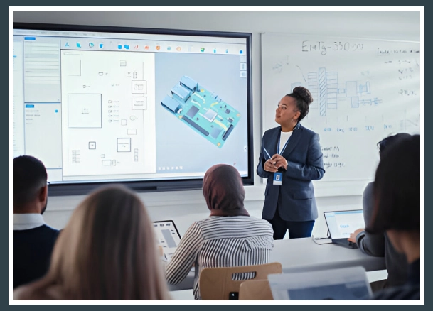
The Fab Virtual Lab enables students to remotely access and control advanced digital design and fabrication tools, bringing cutting-edge technology directly into their classrooms or home computers. Students work with these tools in real-time, guided by expert engineers via video conferencing, allowing for high-precision design, simulation, and prototyping. This network lowers barriers to entry, providing teachers with innovative ways to deliver hands-on, meaningful experiences in fields like engineering, design, and STEM. Fab Virtual Lab fosters technological literacy and inspires the next generation of STEM professionals through live, interactive sessions using state-of-the-art equipment. Activities include virtual workshops, student projects, and interactive labs, all supported by facilitators who help integrate the tools into learning. Surveys show that students find these sessions more engaging than traditional learning, especially among underrepresented groups, sparking greater interest in technology and engineering.
Remote Access Meeting
Investigate
Find the rundown of devices and going with recordings to find what best suits your requirements. You can likewise investigate the aides furnished beneath or make your own with the help of your supplier. Also, look at the Extra Assets to find out about Fab and its contributions.
Plan
Set up your PC. You really want a webcam, mouthpiece, speakers, mouse with scroll wheel, and projector or enormous showcase. Set up a test meeting guarantee all that fills in true to form.Pick your examples. You can involve your own or the supplier’s in-house tests.
Feedback
Educator Overview – enlighten us concerning your experience mentioning, testing, and running remote access. Understudy Review – share this overview with your understudies. We want to find out whether they partook in the experience and thought that it is important.
Accessible Gear Remote Active Control
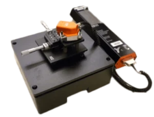
Atomic Force Microscope (AFM)
The nuclear power magnifying instrument (AFM) is one of around two dozen sorts of filtered closeness test magnifying lens. These magnifying instruments work by estimating a nearby property – like level, optical retention, or attraction – with a test or “tip” put exceptionally near the example. The little test partition (on the request for the instrument’s goal) makes it conceivable to take estimations over a little region. To secure a picture the magnifying lens raster-checks the test over the example while estimating the nearby property being referred to. The subsequent picture looks like a picture on a TV screen in that both comprise of many columns or lines of data put one over the other. Suitable for: 9th grade + Remote Access Accessible at: COSINC, SLCC Demo Just Accessible at: CNEU, ECC
Energy-Dispersive X-Ray Spectroscopy (EDS)
Energy-dispersive X-beam spectroscopy (EDS, EDX, or XEDS), at times called energy dispersive X-beam examination (EDXA) or energy dispersive X-beam microanalysis (EDXMA), is an insightful method utilized for the natural investigation or synthetic portrayal of an example. It depends on a cooperation of a few wellspring of X-beam excitation and an example. Its portrayal capacities are to a great extent because of the crucial rule that every component has a novel nuclear construction permitting special arrangement of tops on its X-beam outflow range. Fitting for: 6th grade + Accessible at: ECC
Field Emission Electron Probe Microanalyzer (FE-EPMA)
An electron microprobe (or electron test microanalyzer) is a specific filtering electron magnifying lens, streamlined for exact and exact quantitative compositional examination of strong materials at the small size. It is fundametally equivalent to a SEM, with the additional ability of substance investigation. By utilizing a field discharge type electron weapon, a more modest light source is conceivable and goal is incredibly gotten to the next level. This makes it conceivable to dissect more modest infinitesimal regions. It is utilized for imaging of test morphology and compositional variety, as well as compositional investigation by X-beam spectroscopy with ~1% accuracy. Proper for: 8th grade + Accessible at: Caltech
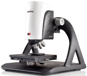
Optical Profiler
An optical profiler is a sort of portrayal hardware utilized for getting real nature 3D information of a surface at the sub-micron level. Optical profilers join key credits of optical magnifying instruments and standard pointer type profilers. An optical profiler accomplishes the genuine nature and wide field of view (FOV) nature of an optical magnifying lens while at the same time getting the nanometer level z-goal of a standard pointer profiling strategy. Suitable for: all grade levels Accessible at: Rio Salado School
Simple to Use, Easy to Access
Designed for students at all levels of education.
Friendly Interface Single point of access for all students wherever they are.
Fast Performance Multiple servers around the world provide ease of access anywhere in the world.
Video Tutorials Video tutorials accessable for all students.
Powerful Options Choose between several tools to get trained and assessed in real time.
Extensions & Addons Several addons and extensions in development for all major browsers.
Expert 24/7 Support Having a problem? Just email us and we will get you sorted out.
Quick, Easy and Secure
No one at FAB Virtual Lab is able to see or modify your personal data. Encrypted servers provide a higher level of protection from end-to-end. We are long Believers of privacy!
Register in 30 Seconds
Click on the link Lets Get Started and easily register with your email once an admin approves your registration, you are all set.
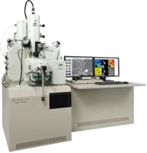
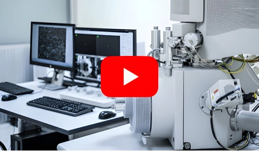
A Checking Electron Magnifying instrument (SEM) is an electron magnifying instrument that creates pictures by filtering an example with an engaged light emission. These electrons associate with the particles of the example, creating signals that uncover insights concerning its surface geology and organization. By examining the electron pillar in a raster design, the place of the shaft is joined with the identified signs to shape a picture. SEMs can accomplish goals of under 1 nanometer and are fit for looking at tests in high vacuum, low vacuum, wet conditions (ecological SEM), and across a scope of cryogenic and raised temperatures. A Field Outflow Examining Electron Magnifying instrument (FESEM) offers a more brilliant electron source and a more modest bar size contrasted with standard SEMs, taking into consideration higher amplification — up to 500,000x. FESEM is particularly helpful for noticing fine surface subtleties, materials delicate to electron radiates, and non-conductive examples, making it ideal for imaging polymers and slight movies. SEM is reasonable for all scholastic levels and can be gotten to at ASU, COSINC, ECC, and SLCC. FESEM is accessible at Caltech, COSINC, and CNEU.
Transmission Electron Microscope (TEM)
An optical profiler is an accuracy instrument used to catch genuine nature 3D surface information at sub-micron levels. It mixes the benefits of optical magnifying lens with those of conventional pointer profilers, offering the wide field of view and genuine nature imaging ordinary of an optical magnifying instrument, while accomplishing the nanometer-level z-goal of a pointer profiler. Appropriate for: Every scholarly level, optical profilers. Accessible for use at: Rio Salado School.
Limited Interaction / Mostly Demonstration
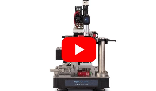
3D Nanoprinter (Lithography)
An optical profiler is a sort of portrayal hardware utilized for getting real nature 3D information of a surface at the sub-micron level. Optical profilers consolidate key ascribes of optical magnifying lens and standard pointer type profilers. An optical profiler accomplishes the genuine nature and wide field of view (FOV) nature of an optical magnifying instrument while at the same time getting the nanometer level z-goal of a standard pointer profiling strategy. Proper for: All grade levels Accessible at: Rio Salado School.
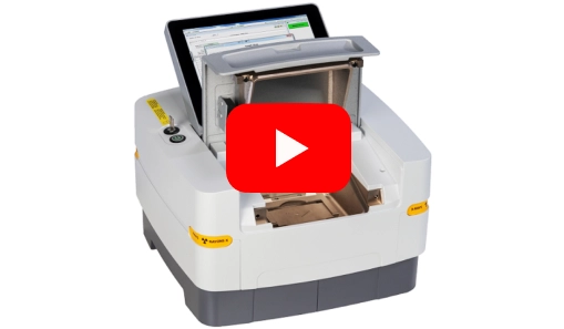
X-Ray Fluorescence (XRF)
An optical profiler is a type of characterization equipment used for obtaining true color 3D data of a surface at the sub-micron level. Optical profilers combine key attributes of optical microscopes and standard stylus-type profilers. An optical profiler achieves the true color and wide field of view (FOV) nature of an optical microscope while simultaneously obtaining the nanometer level z-resolution of a standard stylus profiling technique. Appropriate for: All grade levels Available at: Rio Salado College.
Unleash Your Innovation Potential
Discover limitless opportunities in the world of deep tech.